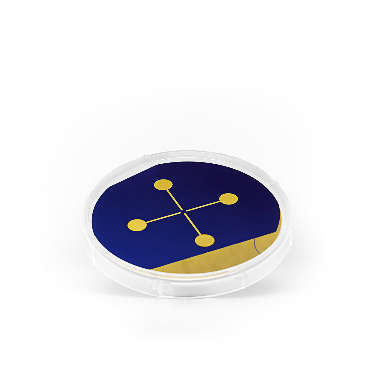
Monolayer Graphene on Cu - Processed in ISO 7 Cleanroom
This product consist on a single-layer graphene grown on copper foil substrate.
Graphene Film
- · Growth method: CVD synthesis
- · Appearance (color): Transparent
- · Transparency: > 97%
- · Coverage: > 95%
- · Number of graphene layers: 1
- · Thickness (theoretical): 0.345 nm
- · AFM Thickness (air @RT): <1nm
- · Electron Mobility on SiO2/Si: ≈1500 cm2/V·s
- · Sheet Resistance on SiO2/Si: 350±40 Ohms/sq (1cm x1cm)
- · Grain size: Up to 20 μm
Substrate Cu Foil
- · Thickness: 18 μm
- · Roughness: around 80 nm
Quality control
All our samples are subjected to a rigorous QC in order to ensure a high quality and reproducibility of the graphene.
- · Raman Spectroscopy on each batch: I(G)/I(2D)<1; I(D)/I(G)<0.1 on 90nm SiO2/Si substrate.
If your application requires more specific controls (AFM, SEM...) please do not hesitate to contact us.
Applications
Flexible batteries, Electronics, Aerospace industry, MEMS and NEMS, Microactuators, Conductive coatings, Research
Publications
“Broadband image sensor array based on graphene–CMOS integration”
Nature Photon 11, 366–371 (2017). https://doi.org/10.1038/nphoton.2017.75
“Selective ion sensing with high resolution large area graphene field effect transistor arrays”
Nat Commun 11, 3226 (2020). https://doi.org/10.1038/s41467-020-16979-y
 Data Sheet Graphene Film
  MSDS Graphene Film