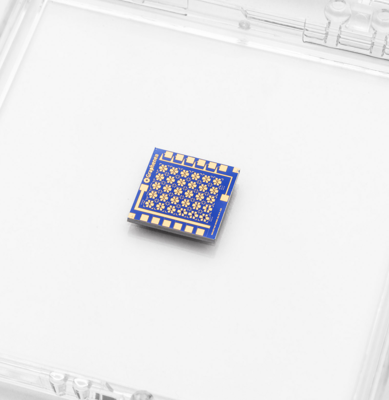

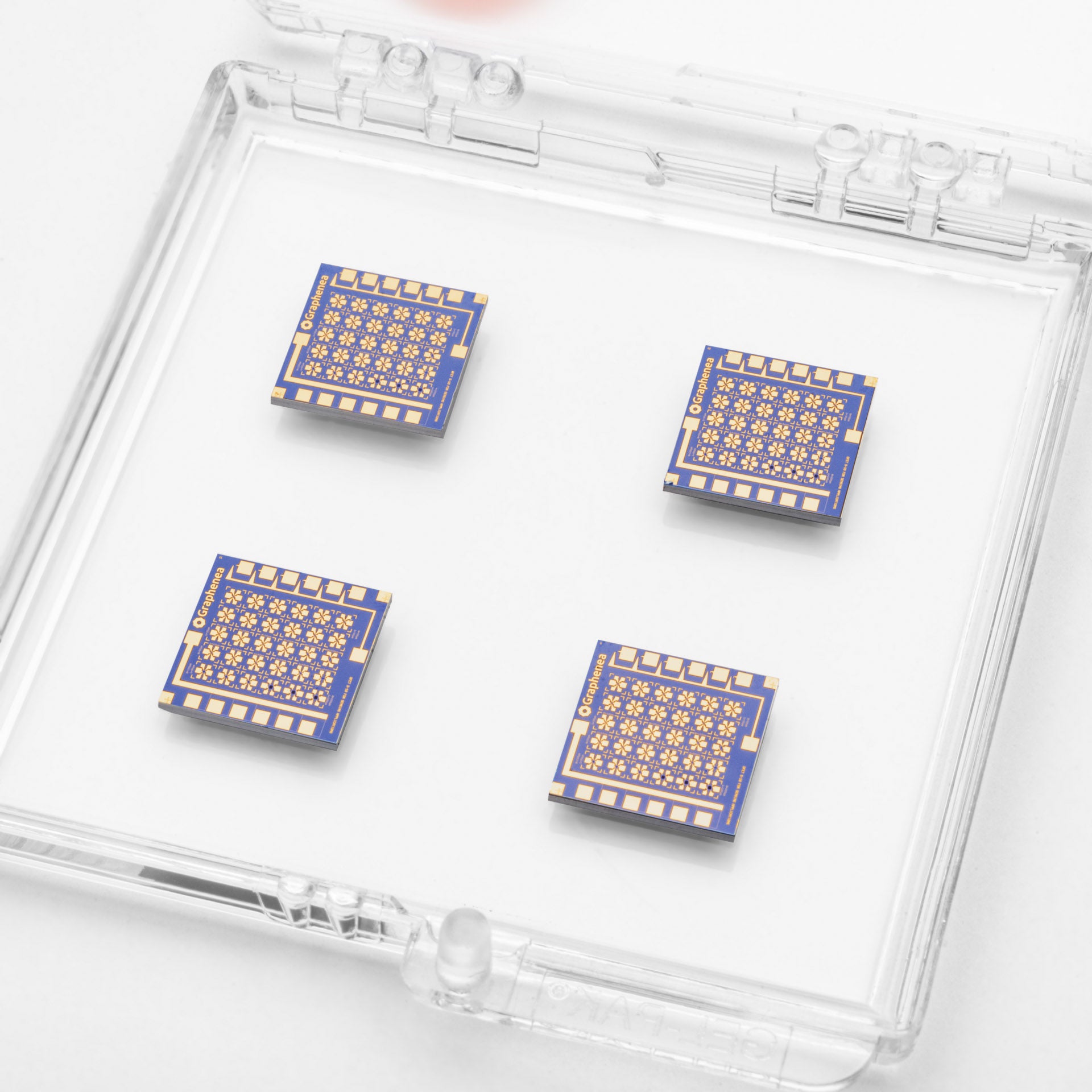


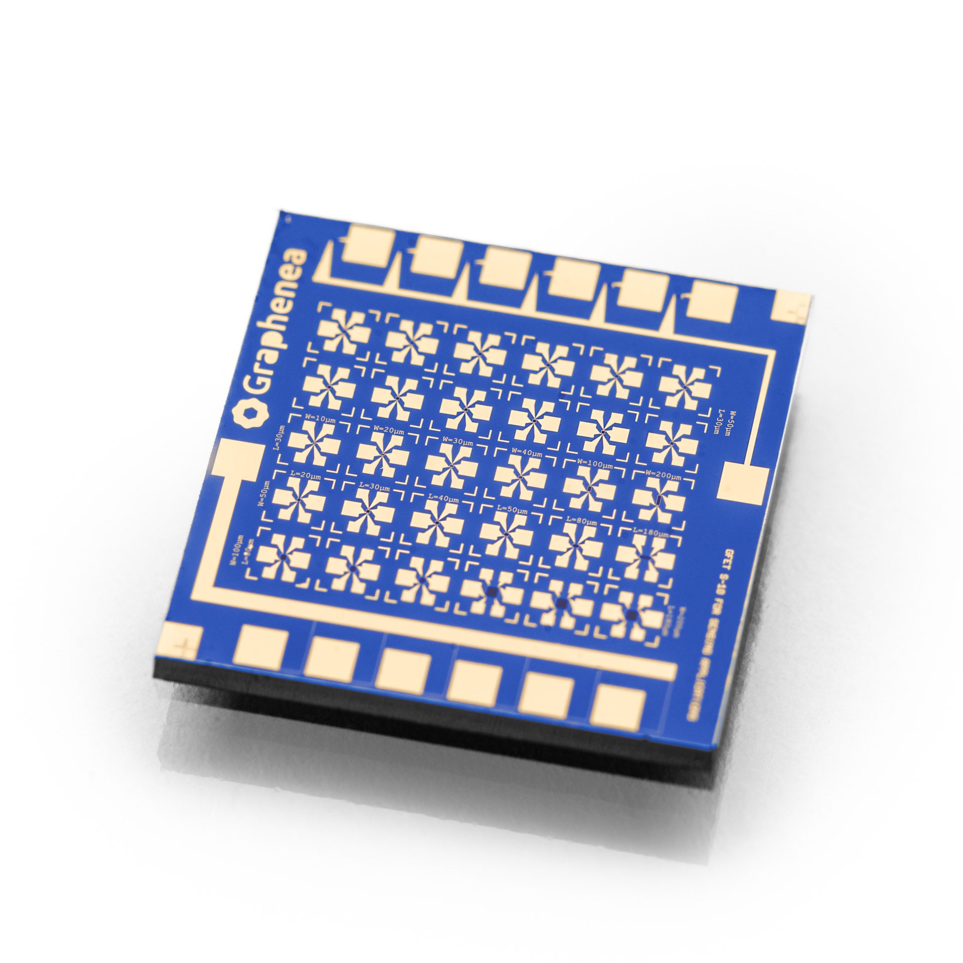
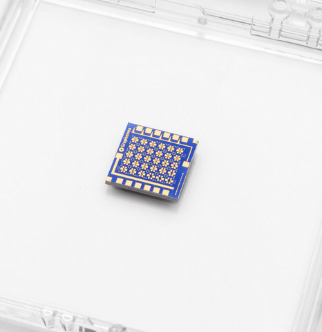


GFET-S10 (Die size 10 mm x 10 mm) - Processed in Clean Room Class 1000
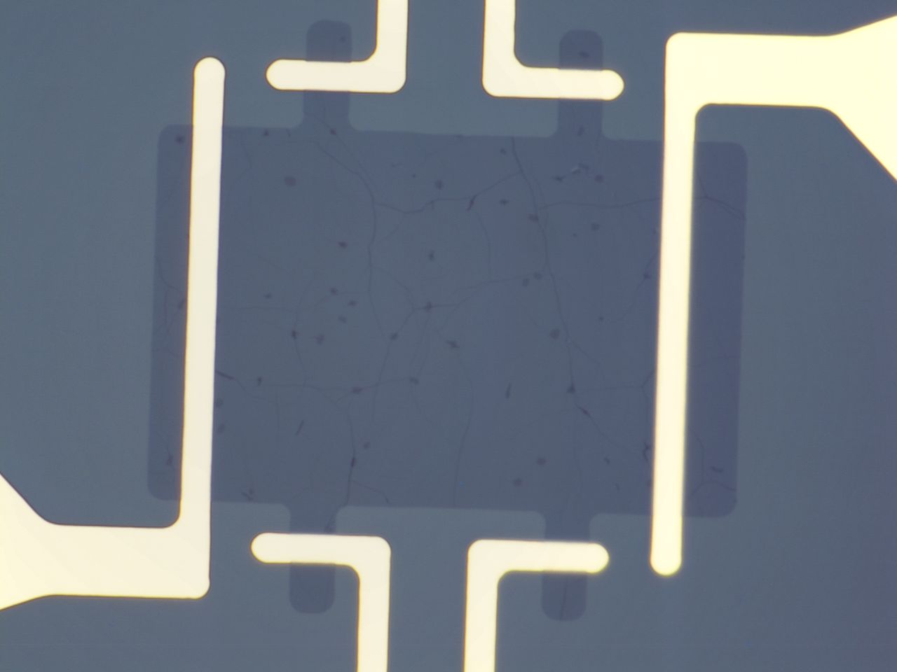
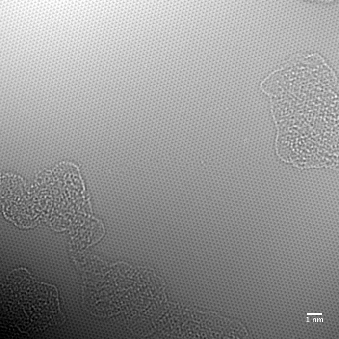
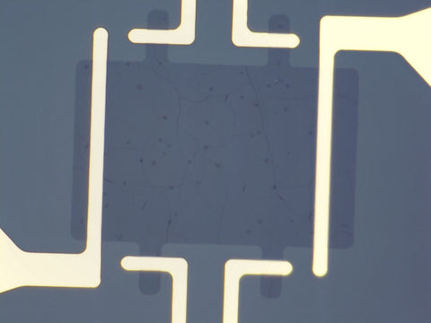
The GFET-S10 chip from Graphenea provides 30 graphene devices distributed in a grid pattern on the chip. Thirty devices have a Hall-bar geometry and six have a 2-probe geometry. The Hall-bar devices can be used for Hall-bar measurements as well as 4-probe and 2-probe devices. There are varying graphene channel dimensions to allow investigation of geometry dependence on device properties.
Typical Specifications
- · Growth method: CVD synthesis
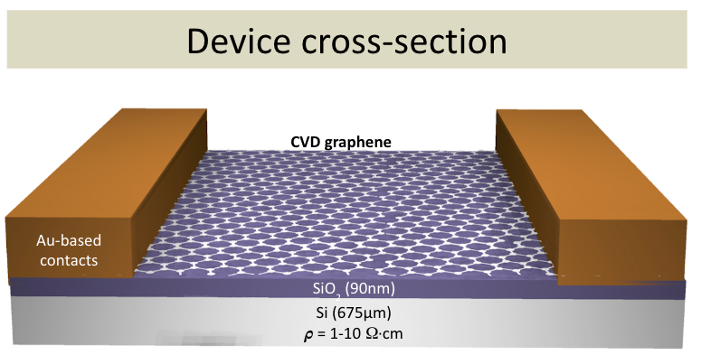
- · Graphene transfer: Polymer assisted transfer
- · Substrate: Si/SiO2
- · Substrate thickness: 675 μm
- · Resistivity of Si substrate: 1-10 Ω.cm
- · Gate oxide thickness: 90 nm
- · Metallization: 50nm Au-based Contacts
- · Chip dimensions: 10 mm x 10 mm
- · Number of GFETs per chip: 30
- · Optical Yield: ≥75%
- · Average field-effect mobility: >1000 cm2/V·s
- · Average Dirac point: <25 V
Absolute maximum ratings
- · Maximum gate-source voltage (back gating): ± 50V
- · Maximum temperature rating: 150 °C
- · Maximum drain-source current density: 107A.cm-2
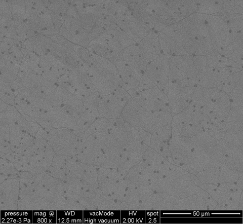
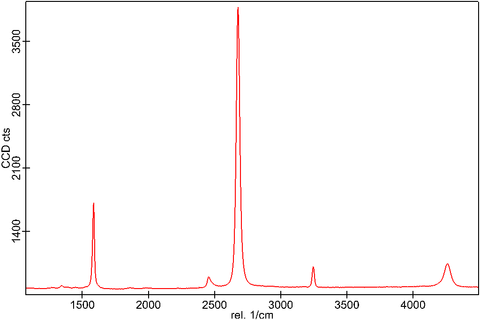
Quality control
All our samples are subjected to a rigorous QC in order to ensure a high quality products.
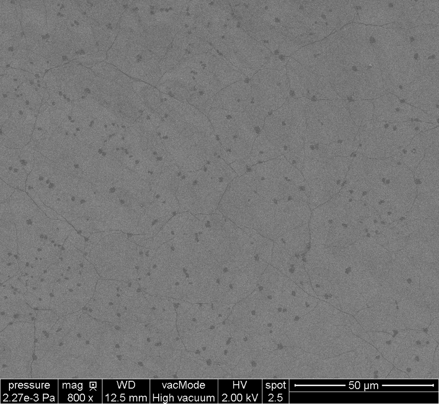
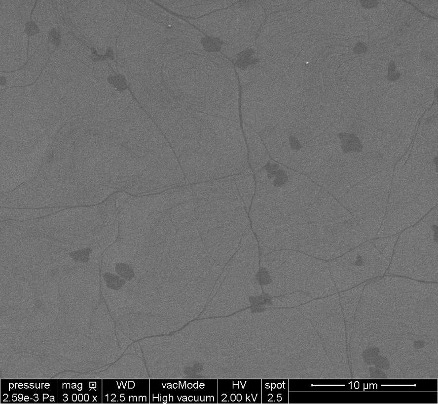
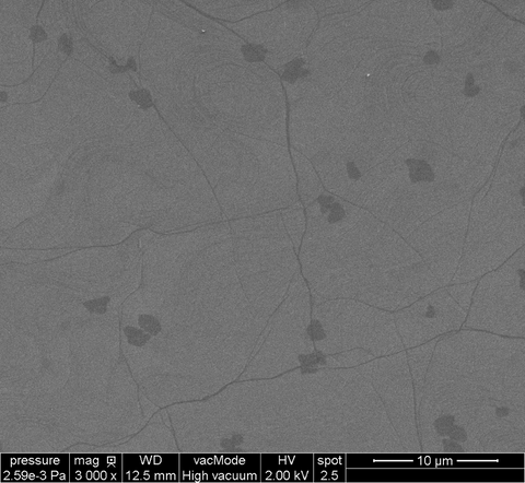
- · Optical microscopy inspection of all the devices
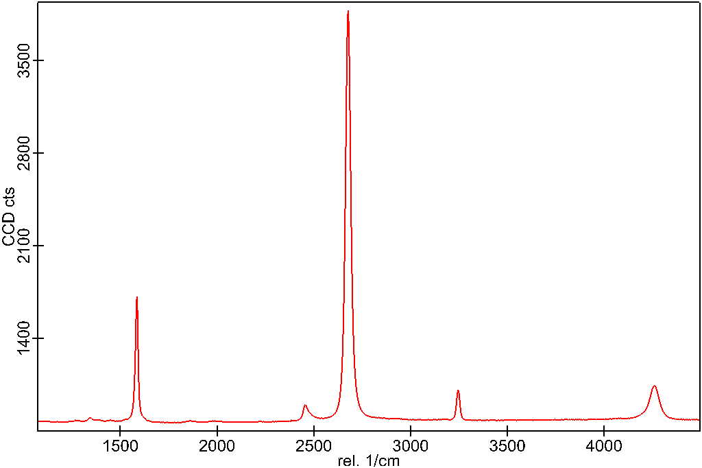
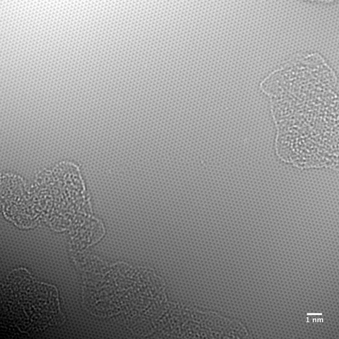
- · Raman Spectroscopy of each fabrication batch
- · Electrical characterization via back gating of each fabrication batch
Applications
Graphene field-effect transistors (GFETs) have unprecedented sensitivity to the surrounding environment and is an ideal transducer for a variety of sensing applications. Depending on the application, GFETs can be tuned to be sensitive only to the stimulus of interest and have shown breakthrough performance in areas such as graphene device research, quantum transport, gas sensors, chemical sensors and magnetic sensors.
Publications
"Graphene field effect transistors on flexible substrate: Stable process and high RF performance"
DOI:10.1109/EuMIC.2016.7777516
"High-Gain Graphene Transistors with a Thin AlOx Top-Gate Oxide"
Scientific Reports volume 7, Article number 2419 (2017) doi:10.1038/s41598-017-02541-2
 GFET-S10 Data Sheet
  Measurements Protocol and Basic Handling Instructions