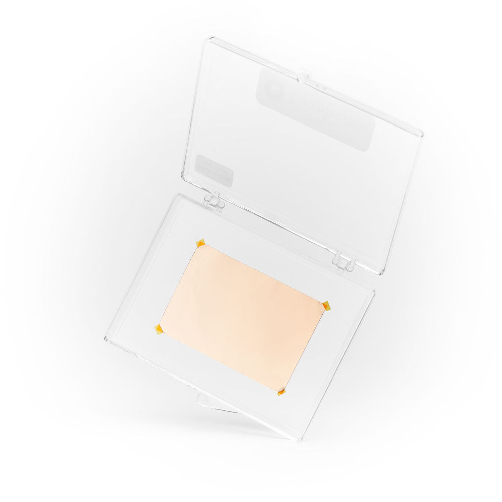


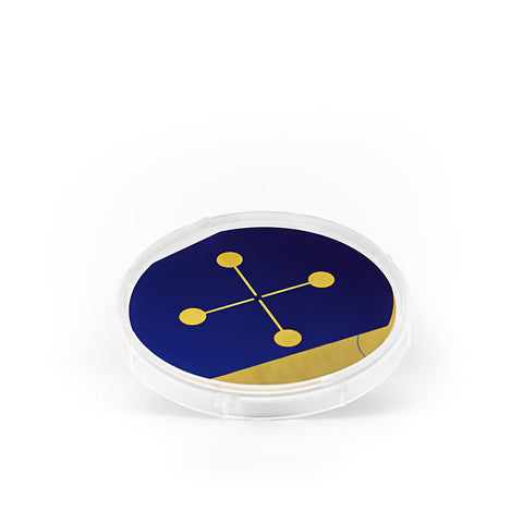
Graphene on Your Substrate - Processed in ISO 7 Cleanroom
This is a tailor made graphene product. You send your substrate to our laboratory (including your order ID and your email address as a reference) and we then use our innovative method to transfer the graphene monolayer on top of it and send it to the address you specify. Examples of substrates we have successfully transferred graphene to: devices, solar cells, LEDs, gold, alumina, silver mirrors and sapphire.
Graphene Film
- · Growth method: CVD synthesis
- · Polymer assisted transfer
- · Appearance (color): Transparent
- · Transparency: > 97%
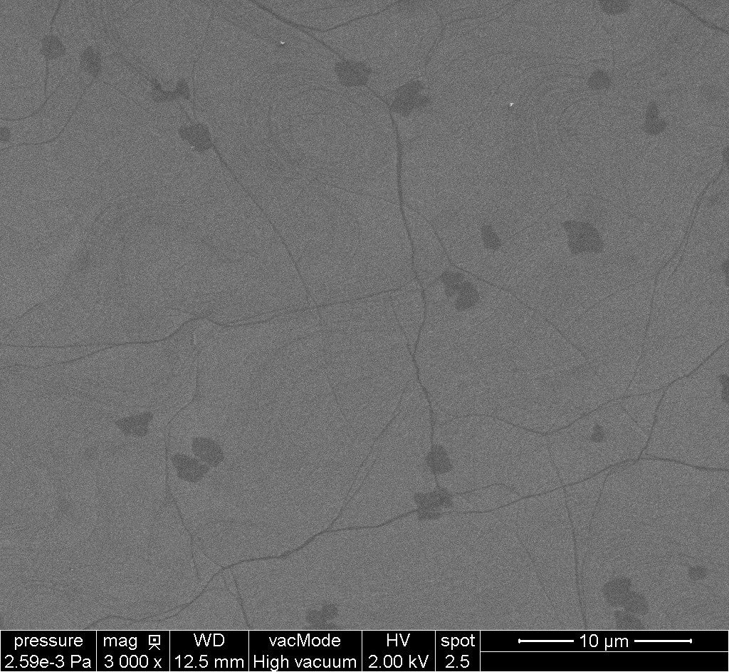
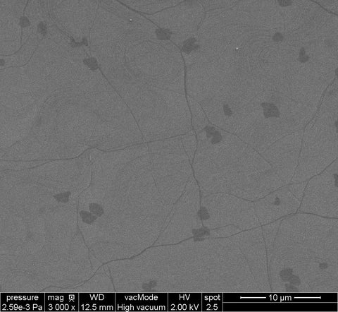
- · Coverage: > 95%
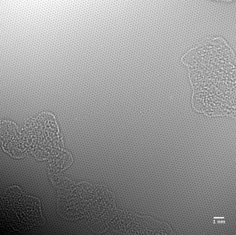
- · Number of graphene layers: 1
- · Thickness (theoretical): 0.345 nm
- · AFM Thickness (air @RT): <1nm
- · Electron Mobility on SiO2/Si: ≈1500 cm2/V·s
- · Sheet Resistance on SiO2/Si: 450±40 Ohms/sq (1cm x1cm)
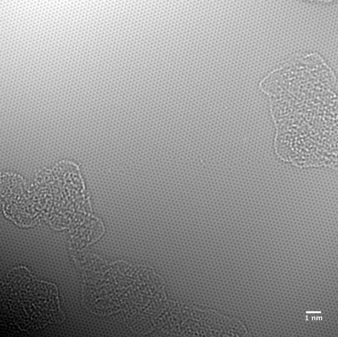
- · Grain size: Up to 20 μm
Quality control
All our samples are subjected to a rigorous QC in order to ensure a high quality and reproducibility of the graphene. All our CVD materials are processed in ISO 7 Cleanroom. Each batch must pass the following tests:
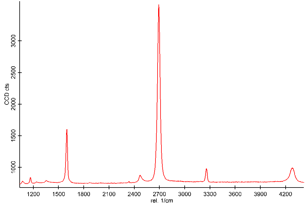
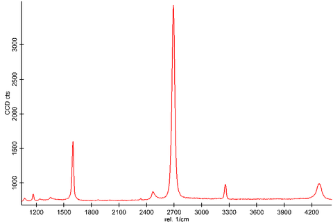
- · Raman Spectroscopy on each batch: I(G)/I(2D)<1; I(D)/I(G)<0.1 on 90nm SiO2/Si substrate.
- · Optical Microscopy inspection of each individual sample to ensure good transfer quality and purity
If your application requires more specific controls (AFM, SEM...) please do not hesitate to contact us.
Publications
“Water Desalination across Nanoporous Graphene”
ACS Publications, Nano Lett., 2012, 12 (7), pp 3602-3608; doi: 10.1021/nl3012853
“Selective Molecular Transport through Intrinsic Defects in a Single Layer of CVD Graphene”
ACS Nano Publications, 2012, 6 (11), pp 10130-10138; doi: 10.1021/nn303869m
“Graphene/Polymer Nanocomposites”
Macromolecules, 2010, 43 (16), pp 6515-6530; doi: 10.1021/ma100572e