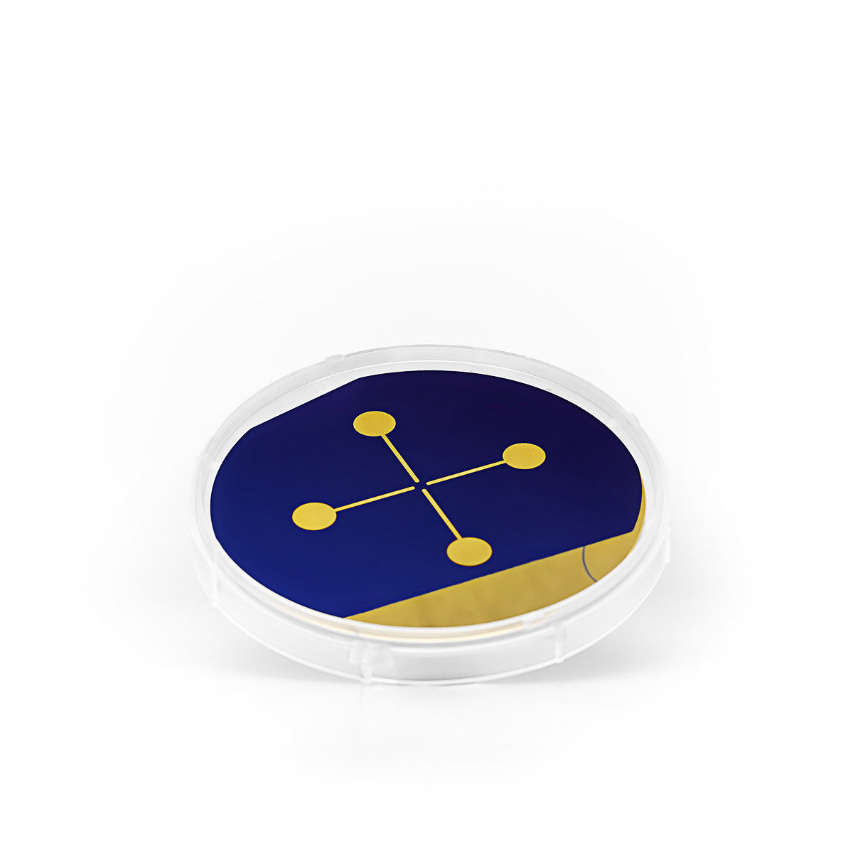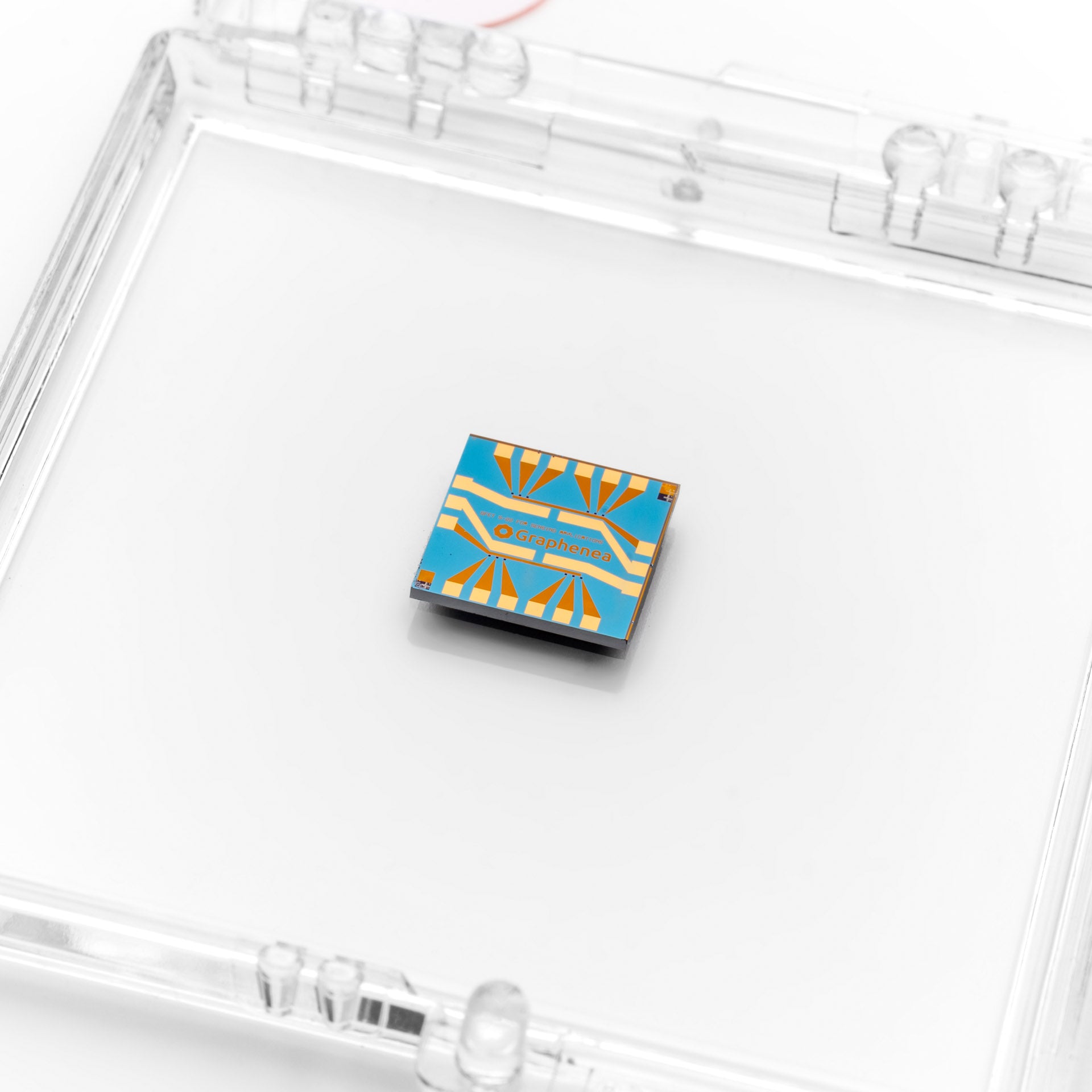

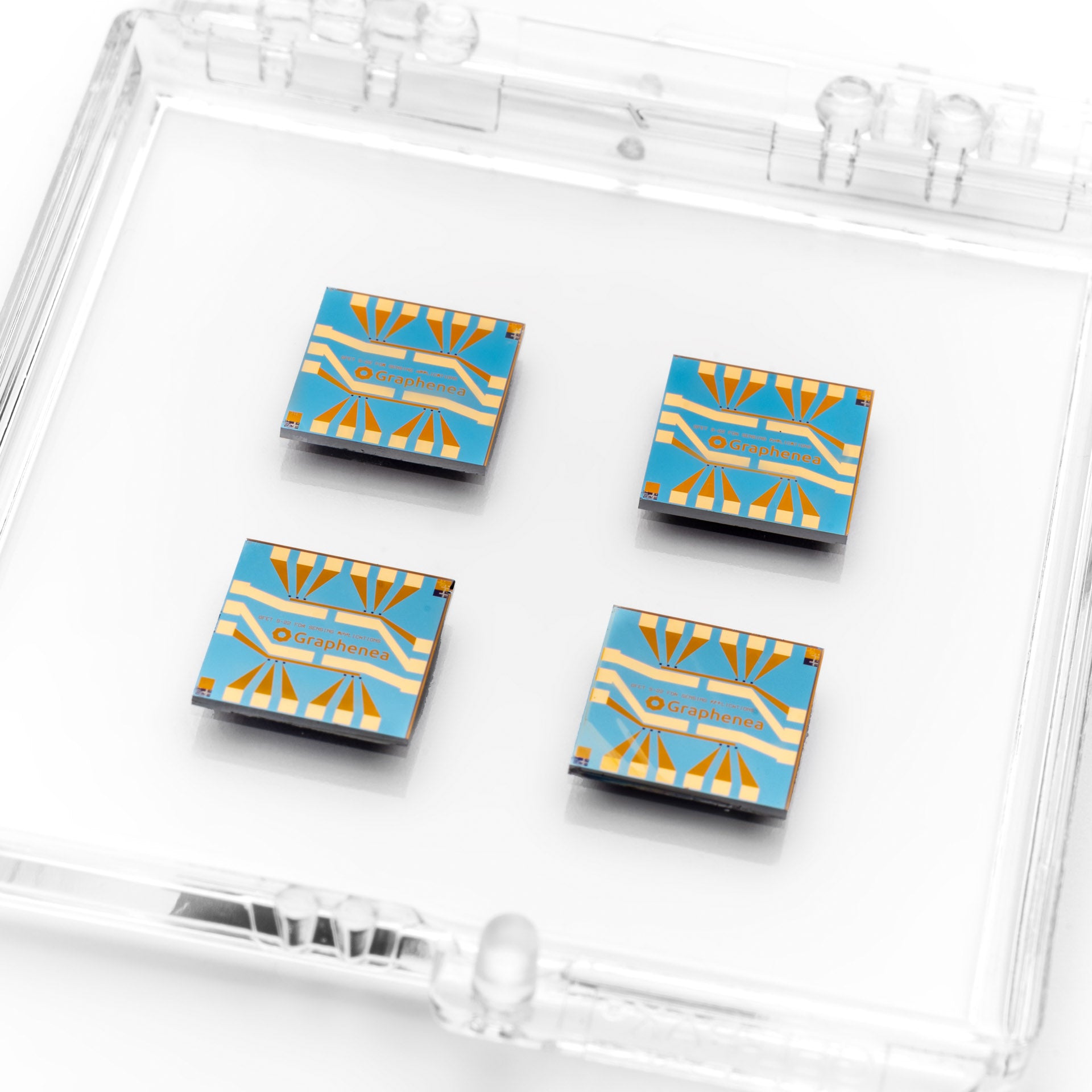


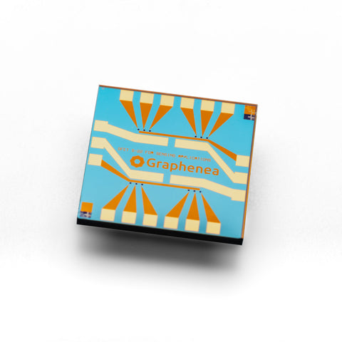
GFET-S22 (Die size 10 mm x 10 mm) - Processed in Clean Room Class 1000
The GFET S-22 chip from Graphenea is designed for measurements in liquid medium. The new version provides 4 independent set of graphene devices, each set with 3 individual channels, with encapsulation on the metal pads to avoid degradation and reduce leakage currents; the probe pads are located near the periphery of the chip. It also includes a non-encapsulated electrode at the center of the chip, which allows liquid gating without the need of an external gate electrode (such as Ag/AgCl probes). This device architecture enables each one of the set of devices to be modified individually, to obtain a multiplexed measurement.
Typical Specifications
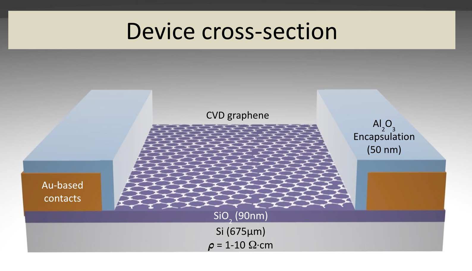
- · Growth method: CVD synthesis
- · Graphene transfer: Polymer assisted transfer
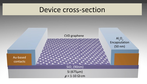
- · Substrate: Si/SiO2
- · Substrate thickness: 675 μm
- · Resistivity of Si substrate: 1-10 Ω.cm
- · Gate oxide thickness: 90 nm
- · Metallization: 50nm Au-based Contacts
- · Encapsulation: 50 nm Al2O3
- · Chip dimensions: 10 mm x 10 mm
- · Number of GFETs per chip: 12 in parallel
- · Number of graphene channels with integrity: ≥9
- · Metallization: Au contacts
- · Average field-effect mobility (back gating): >1000 cm2/V.s
- · Average Dirac point (back gating): <25
Absolute maximum ratings
- · Maximum gate-source voltage (back gating): ± 50V
- · Maximum temperature rating: 150 °C
- · Maximum drain-source current density: 107A.cm-2
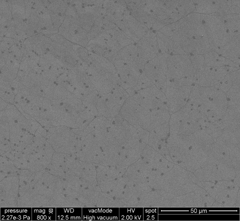
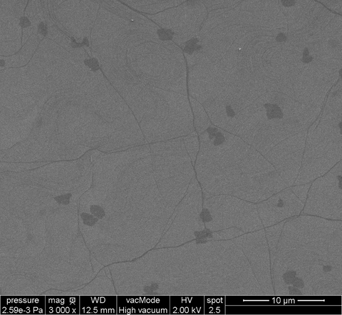
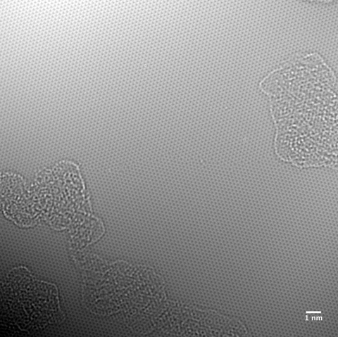
Quality control
All our samples are subjected to a rigorous QC in order to ensure a high quality products.
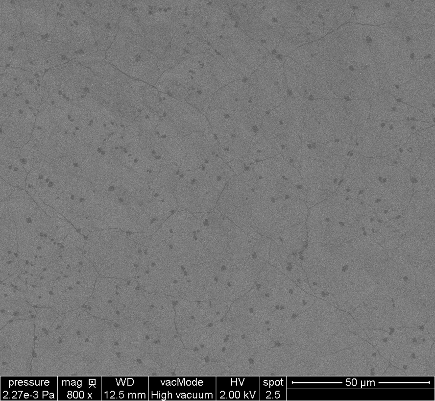
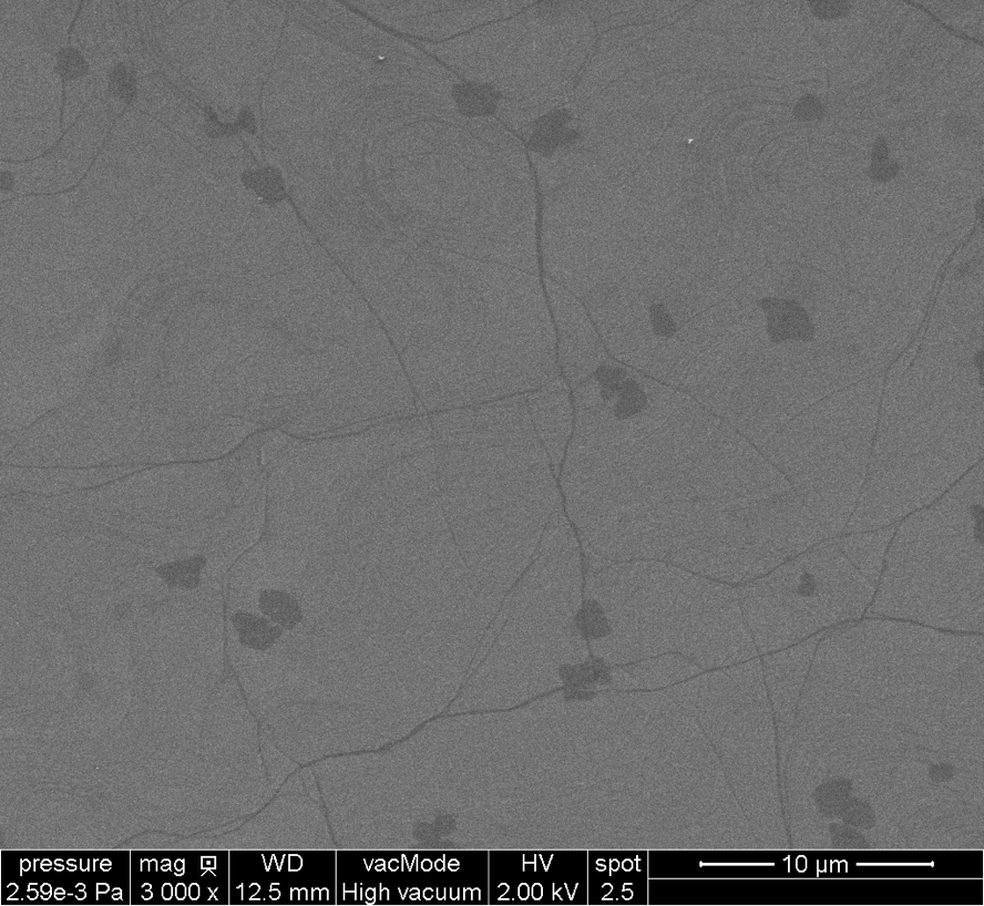
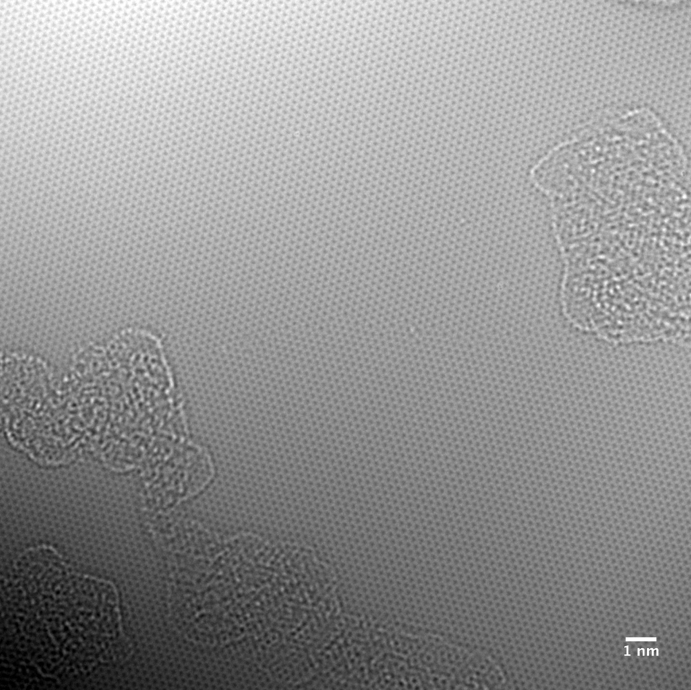
- · Optical Microscopy inspection of all the devices
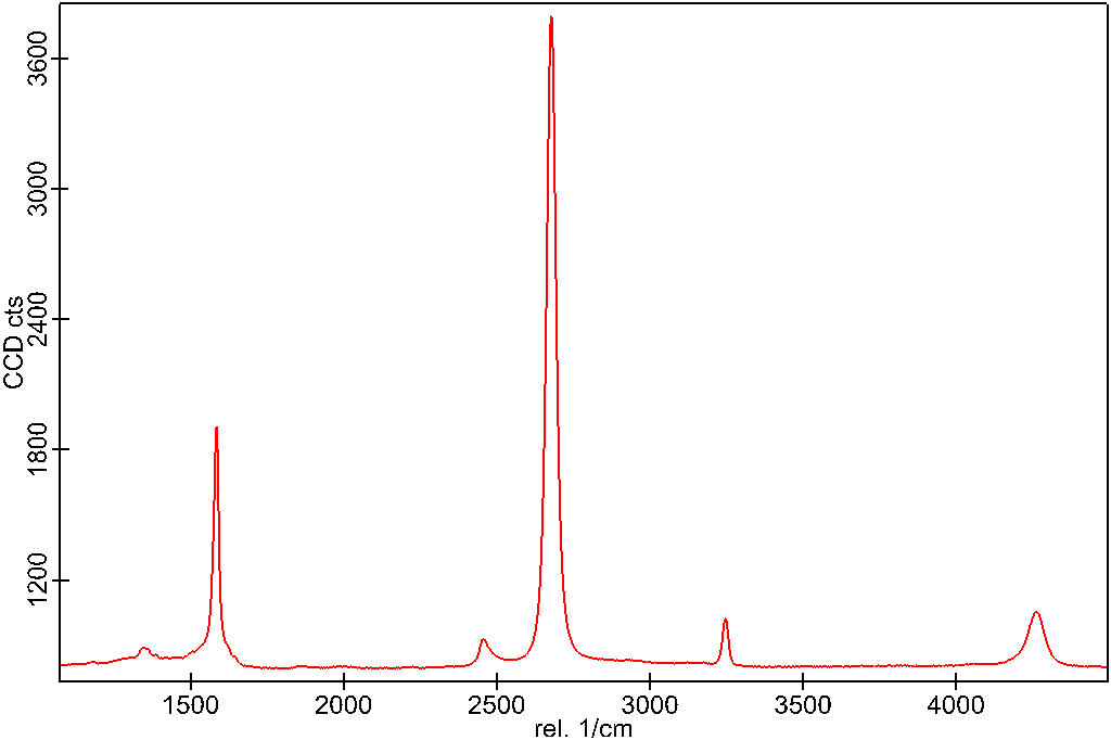
- · Raman spectroscopy of each fabrication batch
- · Electrical characterization via back gating of each fabrication batch
- · AFM of each fabrication batch
Applications
Graphene field-effect transistors (GFETs) have unprecedented sensitivity to the surrounding environment and is an ideal transducer for a variety of sensing applications. Depending on the application, GFETs can be tuned to be sensitive only to the stimulus of interest and have shown breakthrough performance in areas such as graphene device research, chemical sensing, bioelectronics and biosensing.
Publications
"Graphene Sensor Arrays for Rapid and Accurate Detection of Pancreatic Cancer Exosomes in Patients’ Blood Plasma Samples"
https://doi.org/10.1021/acsnano.3c01812
"Graphene‑based field‑effect transistors for biosensing: where is the field heading to?"
https://doi.org/10.1007/s00216-023-04760-1
"Ultrasensitive detection of SARS-CoV-2 spike protein by graphene field-effect transistors"
https://doi.org/10.1039/D2NR05103F
"Detection of Glial Fibrillary Acidic Protein in Patient Plasma Using On-Chip Graphene Field-Effect Biosensors, in Comparison with ELISA and Single-Molecule Array"
https://doi.org/10.1021/acssensors.1c02232
"Detection of an IL-6 Biomarker Using a GFET Platform Developed with a Facile Organic Solvent-Free Aptamer Immobilization Approach"
DOI:10.1109/ACCES.2020.2994611
"High resolution potassium sensing with large area graphene field-effect transistors"
https://doi.org/10.1016/j.snb.2019.04.032
 GFET-S22 Data Sheet
  Measurement Protocols and Basic Handling Instructions